
Printed circuit boards, or PCBs, are so fundamental in electronics, that people often forget to explain what they are. Here, we’re going to break down the mystery and explain what they are, how they’re made and where you will find them.
What is a Printed Circuit Board?
Simply put, a printed circuit board (PCB) provides the base for all the essential electrical components needed to make something work. Through conductive tracks, pads and other features that connect various points together, a PCB allows signals and power to be routed between physical devices. Thus, PCBs provide the foundation that brings electronic components to life and are found in just about every electronic product created.
Still lost? Let’s take a step back and talk about how PCBs came to be.
Where did they come from?
While “printed circuit board” is the most common name, PCBs are also called "printed wiring boards" or "printed wiring cards." These names harken back to how they used to be constructed. Before the current method of making PCBs was developed, their counterparts were constructed through a time-intensive method of point-to-point wiring. All the necessary components were literally wired together and connected in what looked like a big tangled mess.
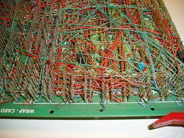
courtesy Wikipedia user Wikinaut<-
This resulted in circuits that were large, heavy, fragile and expensive due to the labor required to make them. Additionally, because everything was connected via wires, as the wire insulation began to age and crack, there were frequently failures at wire junctions that led to short circuits.
Clearly a better method was needed.
As electronics moved from vacuum tubes and relays to silicon and integrated circuits, the size and cost of electronic components began to decrease. Electronics became more prevalent in consumer goods, and the pressure to reduce the size and manufacturing costs of electronic products drove manufacturers to look for better solutions. Thus the modern PCB was born.
What are PCBs Made of?
PCBs consist of multiple layers of materials, each serving a distinct purpose, that are laminated together with heat and adhesive to create a single object - kind of like a lasagna.
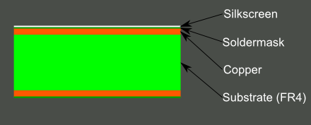
The Base (FR4)
The base material, or substrate, is usually fiberglass, with the most common type being "FR4." While other base materials are used, many lack the durability provided by FR4. This solid core gives the PCB its rigidity and thickness and provides insulation for the other layers. For less rigid PCBs, flexible high-temperature plastic (Kapton or the equivalent) may be used as the base.
Copper
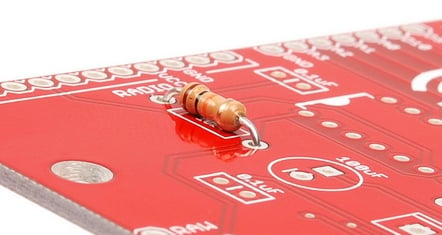
The next layer is a thin copper foil. Depending on the requirements of the PCB, copper may be applied to one or both sides of the substrate. The number of copper layers determines what type of board is created - a double-sided or 2-layer board has copper on both sides of the substrate while a single-sided board only has copper on one side. In typical boards, you will find anywhere from one to 16 layers of copper, though 2 is the most common.
The copper layer(s) provides the conductivity for the PCB. Chemical etching divides the copper into multiple conducting lines, called traces, as well as pads for connections, and other features that make up the base of the circuit on the PCB. The traces take the place of the wires used in older versions and are insulated from one another by air and the substrate material.
Soldermask
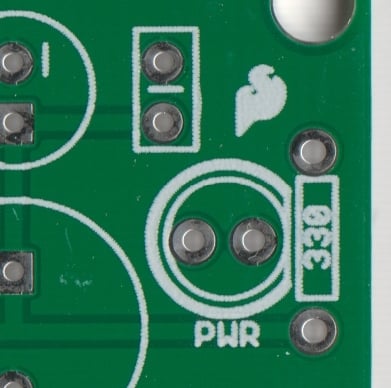
Next comes a layer of soldermask. Soldermask is most commonly green in color but can be almost any color. At SparkFun, we use a red soldermask for most of our boards, purple for LilyPad boards and black for Spark X boards.
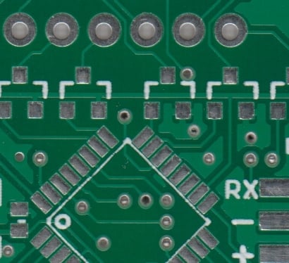
Soldermask is used to insulate the copper traces from accidental contact with other metal, solder or conductive elements. The soldermask covers most of the board, including the small traces, but leaves small rings and pads exposed to allow the user to solder them as necessary.
Silkscreen
On top of the soldermask comes the silkscreen layer. This layer is purely for aesthetics, adding letters, numbers, and symbols to the PCB that allow for easier assembly and make the board easier for humans to understand. The silkscreen is often used to indicate the function of each pin or LED. Silkscreen is most commonly white but any ink color can be used.
What makes a PCB different from a development board?
Now that you have a better understanding of what a PCB is, you may be asking, “but what’s the difference between a PCB and a development board?”
Simply put, development boards (such as Raspberry Pi, micro:bit and Arduino) are PCBS that contain a microprocessor/microcontroller and the minimal support needed for the board to be immediately useful without having to spend time developing additional hardware.
In other words, development boards are PCBs with a little extra hardware and software added in.

What is a